-
- Contact Us
- Privacy Policy
- term and condition
- Cookies policy
MSC360SMA120SD SiC MOSFET: Detailed Specs & Datasheet
SiC MOSFET shipments for industrial power conversion grew more than 30% year-over-year, and the MSC360SMA120SDT arrives as a 1200 V, 360 mΩ SiC MOSFET targeting faster switching and higher-temperature operation. This review is an independent, data-led performance analysis and practical integration guide for engineers evaluating MSC360SMA120SDT for high-frequency power stages and robust thermal environments, combining datasheet-referenced metrics with test recommendations and deployment checklists.
The intent is to give a working engineer a step-by-step evaluation path: key static and dynamic measurements to collect, thermal and layout actions to prioritize, benchmark comparisons to peers, and a production qualification roadmap. Evidence is drawn from the Microchip MSC360SMA120SD(S/C) datasheets and common distributor availability signals; where tests are prescribed, the article lists conditions and expected measurement outcomes so readers can reproduce results in their labs.
H2 1 — Background & device overview (background introduction)
H3 Key specs at a glance
Point: The MSC360SMA120SDT is positioned as a 1200 V SiC MOSFET with a headline Rds(on) of 360 mΩ and recommendations for 18–20 V gate drive, optimized for mid-power industrial converters. Evidence: Microchip datasheets list Vdss = 1200 V, typical Rds(on) = 360 mΩ, package = TO-263-7L-XL and gate-drive recommendation of 18–20 V; rated junction and case temperature ranges are also provided on the official product documentation. Explanation: These specs indicate a device balancing moderate conduction loss with reduced switching energy relative to silicon counterparts; the package choice signals a focus on PCB-mounted power stages where thermal pad area and low parasitic inductance matter. Link: consult the Microchip MSC360SMA120SD series datasheet for parameter tables and typical-characteristic plots when planning tests.
| Parameter | Value |
|---|---|
| Vdss | 1200 V |
| Rds(on) | 360 mΩ (typ) |
| Package | TO-263-7L-XL (D2Pak/variant) |
| Recommended Vgs | 18–20 V |
| Rated temp range | Specified junction range per datasheet; engineered for elevated TJ |
H3 Product family & intended applications
Point: The MSC360SMA120SDT belongs to Microchip's mSiC/MA family aimed at industrial and automotive-adjacent power conversion. Evidence: Product literature groups MSC360SMA120S/D variants with similar 1200 V ratings and Rds(on) targets, intended for PFC, motor drives, on-board chargers (OBC), traction inverters and general-purpose 1200 V stages. Explanation: Within the family, the MSC360SMA120SDT targets designers needing a board-mountable 1200 V SiC MOSFET that trades off slightly higher conduction resistance for compact PCB thermal management and lower switching energy than comparable silicon IGBTs; typical use-cases include high-frequency PFC and OBC front-ends where switching loss dominates and size is constrained. Link: review the family datasheets to select the exact variant for AEC/Q or commercial requirements.
H3 Compliance & options (AEC-Q101, packaging, ordering)
Point: Qualification and packaging variants influence suitability for production and automotive use. Evidence: Microchip lists standard commercial versions and AEC-Q101-qualified options across some mSiC family devices, and major distributors show both tape-and-reel and tray SKUs for board assembly. Explanation: For automotive or harsh-environment applications, choose the AEC-Q101 option where available and plan for additional qualification runs; packaging variants (tape-and-reel vs. bulk) affect assembly throughput and ESD handling. Link: check distributor inventory signals (e.g., Digi-Key, Mouser) and Microchip product pages to assess lead times and alternate sourcing ahead of NPI.
H2 2 — Static & thermal performance (data analysis)
H3 Rds(on) vs. temperature and static conduction behavior
Point: Rds(on) increases with junction temperature; quantifying that slope is essential to estimate conduction losses at operating TJ. Evidence: The datasheet provides Rds(on) vs. TJ curves (typically 25 °C → 150 °C); engineers should digitize or measure that curve to compute I²R losses across operating range. Explanation: Present Rds(on) on the vertical axis and Tj on the horizontal axis; typical table columns to record in lab are: Id (A), Vds (V), measured Rds(on) (Ω), and Tj/Case (°C). For loss budgeting, compute conduction loss as Pcond = I² × Rds(on)_at_TJ × duty; include worst-case at maximum rated TJ and margin for long-term drift. Link: capture both datasheet curves and your own 25–150 °C sweeps to validate batch variation.
H3 Thermal resistance & mounting effects
Point: Thermal path (RthJC, RthJA) and PCB/copper layout dominate steady-state junction temperature under continuous dissipation. Evidence: Use datasheet RthJC estimates and perform board-level RthJA measurements with specified copper areas; thermal modeling should include thermal vias and worst-case ambient. Explanation: Recommended steady-state test points: measure RthJC on a controlled cold-plate, estimate RthJA with board-mounted samples using defined PCB copper areas (e.g., 2–4 in² of 2 oz copper per MOSFET). For thermal modeling, simulate junction rise for expected power dissipation: e.g., 5–10 W localized will drive TJ several tens of degrees depending on copper area and airflow; factor in transient self-heating during repetitive switching. Link: document PCB copper areas, thermal vias, and expected junction rise curves in the design dossier.
H3 Leakage & off-state characteristics
Point: Off-state leakage (Idss) and its temperature dependence determine blocking margin and standby losses. Evidence: Datasheet Idss vs. Vds traces at multiple temperatures are a baseline; measure Idss at room temp and elevated temperatures to determine leakage growth. Explanation: Record Idss at several Vds set points (e.g., 600 V, 800 V, 1200 V) and temperatures (25 °C, 100 °C, 150 °C). For high-voltage designs, leakage at elevated TJ can drive additional dissipation or affect passive clamp behavior; specification margins should guide derating and snubber selection for stable blocking at system voltages.
H2 3 — Dynamic switching metrics & loss analysis (data analysis)
H3 Gate-charge, capacitances and switching-energy tests
Point: Dynamic metrics (Qg, Qgs, Qgd, Coss, Crss) determine required gate-drive sizing and switching energy. Evidence: Standard test conditions should be used: Vds = 400–800 V (or target DC link), Id = representative load (e.g., 10 A), Vgs stepping from 0 → 18 V; record Qg, Qgs, Qgd and measure Coss/Crss at multiple Vds. Explanation: Calculate switching energy by integrating Vds×Id over transition intervals or use Eon/Eoff per-pulse measurements on an oscilloscope; switching loss per second is Psw = (Eon + Eoff) × fsw. Present switching-loss vs. frequency charts to show the crossover where switching loss overtakes conduction loss. Link: include gate-charge curves from the datasheet as initial reference and verify on the actual PCB with the intended gate resistor and driver.
H3 dv/dt, di/dt behavior and safe operating area
Point: Fast SiC transitions create dv/dt and di/dt challenges: overshoot, ringing and potential SOA violations. Evidence: Capture Vds/Id waveforms during turn-on and turn-off with proper probe techniques and a Kelvin-sense arrangement; monitor overshoot amplitude and oscillation frequency as functions of gate resistance and layout. Explanation: Identify required gate resistance to damp oscillations while keeping switching loss acceptable; plot Vds/Id with and without damping to find the sweet spot. Map SOA boundaries for pulsed and repetitive stress to ensure the device does not exceed safe instantaneous power dissipation or charge-related limits in the datasheet. Link: document recommended gate resistor ranges and layout changes that reduce parasitic inductance for production guidance.
H3 Real-world switching loss case (example)
Point: A worked example clarifies relative contributions of conduction vs. switching loss in a 100 kHz half-bridge. Evidence: Example DUT conditions: half-bridge with 400 V DC link, device sees 200 V swing on each leg in hard-switching transitions; assume device Rds(on) = 0.36 Ω, continuous load per device 10 A, measured Eon ≈ 200 µJ, Eoff ≈ 250 µJ (example, verify per-device). Explanation: Conduction loss per device Pcond = I² × Rds(on) × duty = 10² × 0.36 × 0.5 = 18 W. Switching loss Psw = (Eon + Eoff) × fsw = (200e-6 + 250e-6) × 100e3 = 45 W. Total per-device ≈ 63 W; switching dominates (~71%). This demonstrates why SiC MOSFETs are chosen for high-frequency operation despite higher Rds(on): switching loss reductions relative to silicon IGBTs (or different SiC parts) can yield smaller overall system size and higher efficiency. Link: use real measured Eon/Eoff from the lab rather than example numbers when doing a procurement decision.
H2 4 — Benchmarking vs. competitive 1200 V SiC MOSFETs (case + data)
H3 Electrical-performance head-to-head
Point: Standardize a test matrix to compare MSC360SMA120SDT against peer 1200 V, ~360 mΩ parts. Evidence: The matrix should include Rds(on) at 25 °C and 150 °C, Qg (total and split), Coss at multiple Vds, measured Eon/Eoff at a standard Vds/Id, and RthJC. Explanation: A recommended comparison table linearizes differences and highlights trade-offs (lower Qg often correlates with higher Rds(on) or different capacitance profiles). In procurement, require suppliers to provide the same test data and validated samples for cross-testing on your fixture to avoid surprises from differing test methods. Link: use peer datasheets and identical lab conditions to ensure apples-to-apples benchmarking.
| Metric | MSC360SMA120SDT | Peer A | Peer B |
|---|---|---|---|
| Rds(on) @ 25 °C | 360 mΩ | ~300–450 mΩ | ~350–400 mΩ |
| Qg (typ) | Refer to datasheet | Varies | Varies |
| Coss (Vds dependent) | See characteristic curve | See curve | See curve |
| Package | TO-263-7L-XL | TO-247 / D2PAK | TO-263 / SMD options |
H3 Package, thermal and mechanical comparisons
Point: The TO-263-7L-XL package offers a board-mountable profile with lower lead inductance than through-hole TO-247 but less thermal mass. Evidence: Compare thermal pad area, PCB mounting approach and mechanical stiffness; TO-247 often yields lower junction rise under identical cooling due to larger exposed metal and direct heatsink mounting. Explanation: For compact converters where PCB cooling and low loop inductance are prioritized, TO-263-7L-XL is advantageous; for highest continuous power with bulky heatsinks, TO-247/D2PAK may yield easier thermal attachment and lower RthJC. Link: pick package based on your thermal budget and assembly flow, and validate with thermal mapping during prototype tests.
H3 Cost, availability and trade-offs
Point: Procurement decisions must weigh unit cost, lead time and qualification overhead. Evidence: Distributor inventory signals (Mouser, Digi-Key) and Microchip product pages show current stock and common lead-time patterns for mSiC parts; AEC-Q101 variants typically command longer lead times and higher unit cost. Explanation: Trade-offs include accepting slightly higher Qg for lower cost, or choosing a different package to ease thermal design. Maintain alternate suppliers/parts in the BOM and perform lot-to-lot qualification to mitigate supply risk. Link: include distributor lead-time snapshots in the procurement dossier for every new production ramp.
H2 5 — Design & integration best practices (method / how-to)
H3 Gate-drive recommendations & layout rules
Point: Robust gate drive and layout are critical for reliable SiC switching. Evidence: Recommended Vgs(on) is 18–20 V with turn-off to 0 to −3 V depending on system; peak drive currents must support the desired dV/dt while gate resistors damp ringing. Explanation: Specify a gate driver capable of ±4–6 A peak, use a Kelvin gate connection to sense the source near the die, and place the gate loop as small as possible. Suggested gate resistor ranges typically start at 5–22 Ω for damping and increase if EMI or ringing persists; consider split resistors (Rn for turn-on, Rf for turn-off) to tune transitions. PCB checklist: short power loop, generous thermal vias at the package pad, combined gate return and driver ground strategies to avoid common-mode injection into sensitive control circuitry. Link: document gate-drive component values and maintain a lab record of ringing amplitude vs. gate resistor for reproducibility.
H3 Thermal management & reliability-driven derating
Point: Derating and active cooling strategies extend device life and meet reliability targets. Evidence: Apply junction temperature derating rules from the datasheet and industry practice: limit continuous TJ below maximum rated for high-reliability applications and plan margin for ambient variance. Explanation: Use copper pours and thermal vias to spread heat, combine with forced-air cooling or a heatsink where sustained dissipation exceeds PCB cooling capability. Typical guidance: keep TJ under a conservative limit for continuous operation (e.g.,
H3 EMI mitigation & snubber choices
Point: Fast SiC transitions increase conducted and radiated EMI; snubbers and gate damping are primary countermeasures. Evidence: Practical options include RC snubbers across the device, RCD clamps on the bridge, and gate damping to slow edges minimally. Explanation: RC snubbers trade switching energy for reduced dv/dt-induced EMI; RCD clamps capture energy in a controlled path. Gate damping must be tuned to balance increased switching loss vs. reduced EMI; common-mode choke implementation and layout improvements (tight return paths, split grounds) reduce emissions without impacting switching frequency. Link: produce EMI vs. loss trade-off plots for your design choices and include them in the compliance test plan.
H2 6 — Test checklist, qualification path & deployment recommendations (actionable / case-study)
H3 Lab test checklist & pass/fail criteria
Point: A prioritized test checklist speeds evaluation and flags failure modes early. Evidence: Recommended sequence: static IV characterization (Vdss, Rds(on) at multiple Tj), dynamic switching (Qg, Eon/Eoff), thermal cycling (Tj excursions and Rds(on) shift), SOA and avalanche/pulsed stress (if applicable), long-term bias (HTRB/HTOL) and EMI tests. Explanation: For pass/fail, set thresholds such as
H3 Example case study: 10 kW PFC or OBC design using MSC360SMA120SDT
Point: Practical application ties measurement guidance to system-level expectations. Evidence: For a 10 kW OBC with a 400 V DC link, using MSC360SMA120SDT in a bridged stage operating at 100 kHz, designers target switching frequencies that balance thermal dissipation and EMI/size trade-offs; gate resistor and snubber choices stem from lab-tuned damping experiments. Explanation: Expected system-level targets: peak stage efficiency in the high 90s percent (example target ~97–98% depending on topology and losses), per-device thermal dissipation budget informed by measured Pcond and Psw. Learnings: use low-inductance PCB layout, ensure adequate copper for each device thermal pad, and tune gate drive to limit overshoot while achieving acceptable switching loss. Link: replicate the lab measurement matrix in the product qualification plan to ensure repeatable results across assembly lots.
H3 Procurement & qualification checklist for production
Point: Production readiness requires vendor and lot-level controls. Evidence: Steps include verifying AEC-Q101 variant (if required), running incoming lot qualification (sampleed static/dynamic tests), establishing vendor change control, and stocking safety quantities or dual sourcing. Explanation: Recommended minimum DOEs on first article: electrical baseline, thermal cycling, lead-frame/audit checks, and a sample of long-term bias tests. Maintain an approved vendor list and require traceability for wafer lot and assembly lot to meet failure analysis needs. Link: include procurement acceptance criteria and retest intervals in the device management process to reduce field-risk during ramp.
Summary

- The MSC360SMA120SDT is a 1200 V SiC MOSFET with 360 mΩ Rds(on) that favors high-frequency switching applications; engineers should validate both static and dynamic metrics from the Microchip MSC360SMA120SD series datasheet and reproduce Rds(on) vs. TJ curves in their lab.
- Thermal and layout choices (TO-263-7L-XL pad design, copper pours, thermal vias) materially affect steady-state junction temperature—measure RthJA on your PCB and plan cooling for the combined conduction and switching losses.
- Dynamic characterization (Qg, Coss/Crss, Eon/Eoff) and tuned gate damping are essential; in many mid-power half-bridge examples switching losses dominate, so prioritize measured Eon/Eoff and gate-driver capability when selecting MSC360SMA120SDT for 100 kHz+ designs.
- Benchmark against peers with an identical test matrix, include procurement lead-time checks from distributors, and perform lot qualification (thermal cycling, HTOL/HTRB) before volume deployment to ensure reliability and supply continuity.
Frequently Asked Questions
H3 What are the key MSC360SMA120SDT datasheet parameters to verify in initial testing?
Initial testing should verify Vdss at rated voltage, Rds(on) at 25 °C and elevated junction temperatures, gate-charge (Qg, Qgs, Qgd) under datasheet conditions, Coss/Crss vs. Vds, and leakage (Idss) at multiple temperatures. Confirm thermal resistance estimates (RthJC/RthJA) on your PCB and reproduce Eon/Eoff measurements with the intended gate-driver and layout. These checks provide the baseline for conduction and switching loss budgets and guide gate-drive and thermal design choices.
H3 How should an engineer size gate resistors for MSC360SMA120SDT in a 100 kHz half-bridge?
Start with a gate resistor that balances damping and switching loss—typical ranges are 5–22 Ω. Use split resistors (lower on turn-on, higher on turn-off) to tune waveform shape. Measure Vds/Id waveforms while varying resistor values to find the lowest acceptable ringing amplitude and overshoot; target minimal switching loss increase while meeting EMI and voltage-stress constraints. Document final values and retain margin for driver tolerance variation across production lots.
H3 What thermal-management steps are critical for reliable MSC360SMA120SDT operation?
Key steps: maximize PCB copper attached to the package thermal pad with multiple thermal vias, specify forced-air or heatsink options if continuous dissipation exceeds PCB capabilities, measure RthJA on the actual board, and derate continuous TJ per your reliability target (use conservative TJ limits for long life). Perform thermal cycling and high-temperature bias tests (e.g., HTOL/HTRB) to verify no excessive drift in Rds(on) or leakage across production lots.
H3 How does MSC360SMA120SDT compare to TO-247 SiC parts for high-power applications?
The TO-263-7L-XL MSC360SMA120SDT offers lower loop inductance and PCB-mount convenience relative to TO-247, but TO-247 variants often provide lower RthJC and easier heatsink attachment for highest continuous power. Choose MSC360SMA120SDT when board-level cooling and compactness are priorities; prefer TO-247 style packages when maximum sustained dissipation and simple heatsink mounting dominate the design trade-offs.
H3 What procurement and qualification steps minimize supply risk when adopting MSC360SMA120SDT?
Require AEC-Q101 variants if automotive-grade reliability is needed, run incoming lot qualification with static/dynamic tests, maintain dual-source options or alternate BOMs, and set minimum stocking levels for ramp. Include vendor change control clauses and request traceability to wafer and assembly lots. Finally, capture distributor lead-time snapshots (e.g., Mouser, Digi-Key) during NPI to plan safety stock and mitigate ramp-related shortages.
- Technical Features of PMIC DC-DC Switching Regulator TPS54202DDCR
- STM32F030K6T6: A High-Performance Core Component for Embedded Systems
- MSC080SMA330D/S: 3300V SiC MOSFET Data Report
- MSC400SMA330D/S: 3300V SiC MOSFET Specs; Data-Driven Review
- MSC400SMA330D/S: 3300V SiC MOSFET Specs; Data-Driven Review
- MSC400SMA330D/S: 3300V SiC MOSFET Specs; Data-Driven Review
- 3300V SiC MOSFET MSC025SMA330D/S-P01 US Market Data Insights
- 3300V SiC MOSFET MSC025SMA330D/S-P01 US Market Data Insights
- 3300V SiC MOSFET MSC025SMA330D/S-P01 US Market Data Insights
- 3300V SiC MOSFET MSC025SMA330D/S-P01 US Market Data Insights
-
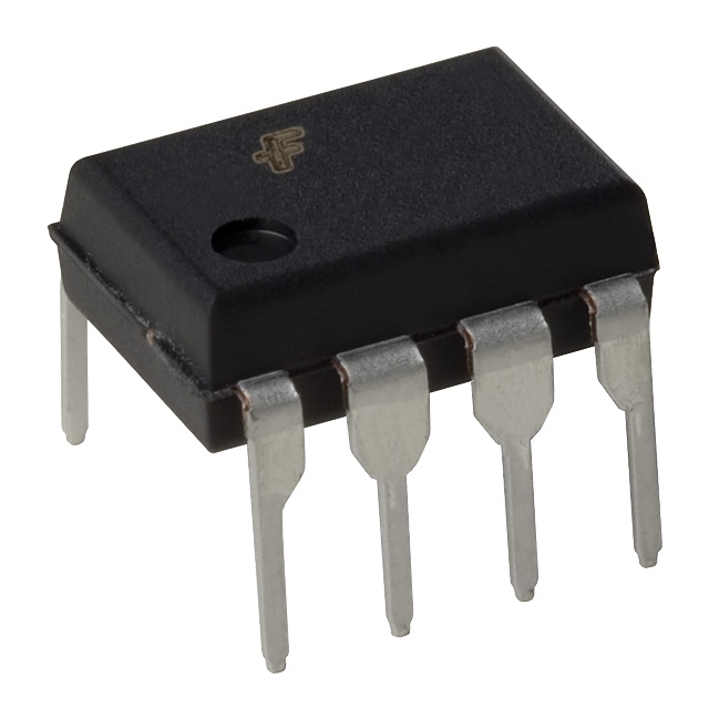 HCPL2601onsemiOPTOISO 2.5KV OPN COLL 8-DIP
 -
 MCT6onsemiOPTOISOLATOR 5KV 2CH TRANS 8-DIP
 -
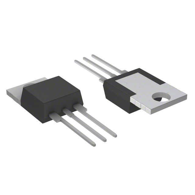 S6008LLittelfuse Inc.SCR 600V 8A TO220
 -
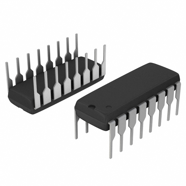 MM74HC4050NonsemiIC BUFFER NON-INVERT 6V 16-PDIP
 -
 MM74HC4049NonsemiIC BUFFER NON-INVERT 6V 16-PDIP
 -
 MM74HC4040NonsemiIC BINARY COUNTER 12-BIT 16DIP
 -
 MM74HC4020NonsemiIC BINARY COUNTER 14-BIT 16DIP
 -
 MM74HC393NonsemiIC BINARY COUNTR DL 4BIT 14MDIP
 -
 MM74HC374NonsemiIC FF D-TYPE SINGLE 8BIT 20PDIP
 -
 MM74HC373NonsemiIC D-TYPE TRANSP 8:8 20-PDIP


