-
- Contact Us
- Privacy Policy
- term and condition
- Cookies policy
MSC030SMB120B4N SiC MOSFET Performance Report: Metrics
Introduction
Point: The is specified as a 1,200 V silicon‑carbide (SiC) N‑channel MOSFET with a typical RDS(on) of 30 mΩ at VGS = 18 V — a specification that yields measurable efficiency gains in high‑voltage power stages when correctly implemented. Evidence: this rating and the 30 mΩ typical RDS(on) value are stated in the device datasheet (Microchip / ). Explanation: for US power‑conversion engineers, that combination (high blocking voltage plus low on‑resistance) reduces conduction loss at medium–high currents and enables higher switching frequencies relative to comparable silicon MOSFETs. Link: engineers should reference the datasheet for tolerance tables and the manufacturer’s recommended operating conditions when translating these sheet numbers into thermal and efficiency budgets.
— Key specs & market context
 — Key specs & market context">
Electrical ratings and key datasheet numbers
Point: The datasheet lists the baseline electrical ratings that determine suitability across high‑voltage applications: VDS = 1200 V and a low typical RDS(on) = 30 mΩ at VGS = 18 V. Evidence: the manufacturer’s product documentation provides continuous and pulse drain current limits, RDS(on) typical and maximum values at specified gate voltages, VGS operating range, threshold voltage, and avalanche/pulse ratings. Explanation: typical use numbers an engineer will extract from the sheet include continuous drain current (case‑limited, e.g., nominally tens of amps in a TO‑247 package), pulse current ratings for short bursts, RDS(on) at both 18 V and 15 V gate drive (the 18 V value is the specified typical), VGS recommended operating range and safe threshold windows for hard switching. Practical note: when converting datasheet numbers into design margins, always use the maximum RDS(on) and high‑temperature curves for worst‑case conduction loss, and apply the supplier’s stated tolerances for RDS(on) and Vth when specifying acceptance tests.
Package, thermal limits, and pinout (TO‑247 4‑lead, source‑sense)
Point: is supplied in a TO‑247 4‑lead package with a Kelvin source lead (source‑sense) that separates the current‑carrying source from the gate drive return. Evidence: the package details and recommended mounting torque/thermal resistance guidance appear in the official package information in the product documentation. Explanation: the TO‑247 4‑lead form factor enables lower measured RDS(on) by using a Kelvin connection for the gate‑drive return, reduces apparent loop inductance between gate and source measurements, and facilitates more accurate on‑resistance and switching characterization. Thermal resistance (RthJC and RthJA) for the package governs junction temperature rise for a given package‑to‑heatsink chain; mounting practices, flatness, torque, and TIM choice all materially affect the achievable RthCA (case‑to‑ambient via heatsink). Link: apply the datasheet’s RthJC number plus measured case‑to‑heatsink thermal resistance to predict junction temperature under continuous and pulsed conditions.
Target applications and value proposition in US markets
Point: Primary US use cases are EV traction inverters, solar and utility inverters, industrial motor drives, and high‑density power supplies where high blocking voltage, low conduction loss, and fast switching are required. Evidence: industry trend reports and the device positioning in distributor listings place this part against competing 1200 V SiC discretes. Explanation: for EV traction inverters and high‑power industrial drives, switching loss and thermal management dominate system design; the ’s low RDS(on) reduces conduction losses at medium to high currents, and its SiC switching characteristics permit higher switching frequency or reduced passive size. For grid‑tied inverters and power supplies, switching energy, device ruggedness, and thermal margin drive system reliability and cost decisions.
Performance Metrics (on‑state, switching, thermal)
 Performance Metrics (on‑state, switching, thermal)">
On‑state conduction: RDS(on) vs VGS & temperature
Point: Conduction loss is Pcond = I² × RDS(on); RDS(on) depends strongly on VGS and junction temperature. Evidence: the datasheet provides RDS(on) vs. VGS curves and RDS(on) vs. Tj derating data; reference device characterization literature for SiC shows RDS(on) increases with Tj. Explanation: use the datasheet RDS(on) at 18 V as the baseline (30 mΩ typical). Example numeric calculation: at I = 50 A, Pcond = 50² × 0.03 = 75 W per device (steady state at the quoted RDS(on)). If RDS(on) doubles at elevated junction temperature (common for wide‑bandgap devices over the full Tj swing), Pcond would be 150 W at the same current — demonstrating the importance of thermal control. Practical equation for temperature scaling: RDS(on,T) ≈ RDS(on,25°C) × (1 + α × (Tj − 25°C)), where α is extracted from the vendor curve; use the vendor curve rather than a single α when available.
Switching performance: rise/fall times, Eon/Eoff, and dynamic losses
Point: Switching energy per transition (Eon, Eoff) and gate charge (Qg) govern dynamic loss and determine usable switching frequency: Psw ≈ (Eon + Eoff) × fsw. Evidence: double‑pulse test (DPT) results in the vendor datasheet or lab reports provide Eon/Eoff at specified conditions; device Coss, Crss, and Qg are published. Explanation: measure switching energy with a standardized double‑pulse test and report energies at controlled VDS, ID, VGS and gate‑drive conditions. Example: if Eon + Eoff = 1.2 mJ at a given VDS/ID and switching slope, at fsw = 50 kHz Psw ≈ 60 W. Gate‑drive power is Pg = Qg × Vdrive × fsw (e.g., Qg = 40 nC, Vdrive = 18 V at 50 kHz → Pg = 36 W). These numbers illustrate that at medium‑to‑high switching frequencies, switching and gate losses can rival conduction losses; optimizing gate drive and dead‑time is therefore essential.
Thermal behavior and Safe Operating Area (SOA)
Point: Junction temperature under combined conduction and switching loss must remain below the datasheet Tj(max); SOA curves and RthJC determine allowable continuous and pulsed currents. Evidence: the datasheet provides RthJC, thermal limits, and SOA/pulse tables; reliability studies on 1200 V SiC MOSFETs show sensitivity to thermal cycling and peak junction stress. Explanation: calculate steady‑state junction temperature as Tj = Ta + Ptotal × RthJA (or Tj = Tc + Ptotal × RthJC where Tc is measured case temperature). Example: for Ptotal = 100 W and RthJC = 0.4 °C/W (typical for a well‑mounted TO‑247), the junction‑to‑case rise is 40 °C; add case‑to‑ambient via heatsink to determine Tj. For pulsed operation, use thermal impedance and energy‑to‑temperature conversions to model transient Tj excursions and verify SOA margins against the vendor pulse/energy curves.
Benchmarking methodology & test setup (standardized, reproducible)

Standard test conditions and normalization
Point: Use a consistent set of test points for cross‑device comparability: VDS (e.g., 600 V for half the rating and 1,200 V for full), VGS = 15 V and 18 V, Tj points at 25 °C and 150 °C, and representative pulse widths for DPT. Evidence: standard industry practice (double‑pulse, pulsed ID, and steady‑state conduction checks) and published test reports recommend these points for 1200 V SiC comparatives. Explanation: recommended normalization table (example columns): Test ID, VDS, ID (pulse/steady), VGS, Tj, pulse width, duty, measurement bandwidth. Use the same PCB fixture, same Kelvin wiring, and consistent probe types so results are comparable between devices. Normalizing Eon/Eoff to per‑mm² or per‑package metrics (see next subsection) improves fairness across die sizes and packages.
Measurement equipment, waveforms, and best practices
Point: Accurate switching and RDS(on) measurements require high‑bandwidth scopes, low‑inductance current probes, isolated gate drives, and optimized layout. Evidence: measurement best practices from lab references and the device datasheet emphasize Kelvin source connections and short loop inductance for reliable DPT results. Explanation: checklist to minimize error: use >200 MHz bandwidth scope for fast edges, wideband differential/ Rogowski current probes for high di/dt, Kelvin source for RDS(on) measurement, short gate/source leads (
Data processing, reporting formats, and comparison metrics
Point: Standardized CSV formats and visualization conventions make device comparisons reproducible and transparent. Evidence: vendors and benchmarking groups publish CSV schemas for RDS(on) sweeps, Eon/Eoff tables, and thermal test logs. Explanation: recommended CSV column set: test_id, device, package, VDS, ID, VGS, Tj, pulse_width_us, Eon_mJ, Eoff_mJ, Qg_nC, Coss_pF, RDSon_mOhm, measurement_notes. Visualizations: normalized loss vs. current curves, efficiency vs. load, and junction temperature vs. time plots. When reporting Eon/Eoff, normalize to per‑package or per‑mm² of die to account for die‑size advantages when comparing parts.
Comparative benchmarks & application case studies

Lab comparison vs competing SiC devices and high‑voltage Si MOSFETs
Point: Head‑to‑head testing must hold package, fixture, and test conditions constant to highlight intrinsic device advantages. Evidence: published comparative studies for 1200 V SiC show consistent switching and efficiency advantages over silicon MOSFETs under the same conditions. Explanation: prioritize KPIs: efficiency at defined load points (10%, 50%, 90%), total device loss (conduction + switching + gate), thermal rise on a common heat sink, and switching‑induced EMI. Report absolute and normalized metrics (per mm² or per package). For example, a SiC device with 30 mΩ RDS(on) and 1.0 mJ switching energy will typically show a multi‑percent efficiency improvement at 10 kW vs a silicon MOSFET with higher switching energy, especially at higher switching frequencies.
Real‑world system case: 10 kW inverter example
Point: A worked 10 kW inverter example quantifies system benefits when replacing a silicon MOSFET with . Evidence: use the device’s conduction and switching characteristics plus typical inverter operating points. Explanation: assume half‑bridge per phase, DC bus 600–700 V, average leg current for 10 kW ~ 12–20 A RMS per leg depending on topology. Using earlier loss approximations (conduction + switching), compute per‑device loss and scale to system. Example simplified result: with reduced switching energy and lower RDS(on), system efficiency improves by 0.5–2.0 percentage points depending on switching frequency and load profile; reduced passive size (smaller inductors/filters) and improved thermal margin permit smaller heat sinks and potentially lower system cost. Include a minimal BOM: devices, gate drivers, Kelvin‑wiring PCB, snubbers, heat sink, TIM, mounting hardware.
Reliability & accelerated testing insights
Point: Key failure modes include thermal cycling fatigue, gate‑oxide degradation, and avalanche/power‑cycling stress; accelerated tests should be requested. Evidence: reliability characterization studies for 1200 V SiC MOSFETs and industry HTRB/HTOL guidance identify these stressors. Explanation: ask suppliers for results of HTRB/H3TRB, high‑temperature reverse bias, and power‑cycling tests relevant to expected junction temperature swings. For procurement, specify acceptable drift limits for RDS(on) and threshold shifts after accelerated stress; require traceable lot data and sample qualification runs to validate long‑term performance in the intended application environment.
Design optimization & procurement checklist (practical actions)

Gate drive, layout, and EMI mitigation
Point: Proper gate drive and PCB layout minimize overshoot, ringing, and EMI while controlling switching losses. Evidence: device gate charge and recommended gate drive circuits in vendor application notes show start‑point component values. Explanation and practical starts: choose gate resistors in the 5–20 Ω range as a starting point (lower for faster switching where layout inductance is minimized; higher where EMI must be controlled). Use a negative‑VGS clamp (≈ −2 V) to prevent gate oscillation, and implement a Kelvin source connection for the gate driver return to avoid shared current‑return loops. Layout do’s: minimize the power loop area, place DC link capacitor close to the switch, and route gate traces away from high‑di/dt paths. Add RC snubbers or RCD clamps where unavoidable energy needs to be absorbed.
Thermal management and mechanical assembly
Point: Heatsink sizing and correct mechanical assembly determine the practical continuous current capability of the TO‑247 device. Evidence: thermal resistance numbers (RthJC) in the datasheet and package mounting guidance should be combined with calculated device losses. Explanation and calculation: given a predicted device loss Pdev, required heatsink thermal resistance RthA_required = (Tj_max − Ta_max)/Pdev − RthJC − RthCH, where RthCH is case‑to‑heatsink thermal resistance including TIM. Typical TO‑247 bolt torque is around 6–8 in‑lb (0.7–0.9 N·m) with a flat, clean mounting surface and a thin, high‑performance TIM (e.g., thermal grease or phase‑change pad). Validate thermal interface by measuring Tc under representative load and using thermocouples at case and heatsink.
Procurement, qualification, and long‑term sourcing tips
Point: A structured incoming inspection and qualification plan reduces risk from counterfeit or out‑of‑spec parts. Evidence: distributor and manufacturer traceability recommendations and acceptance test best practices. Explanation: procurement checklist: order from authorized distributors, request lot traceability and quality certificates, retain sample parts for long‑term reference. Incoming test plan (minimum): visual/package inspection, basic IV sweep, spot RDS(on) measurement at controlled VGS and Tcase for a sample subset, and gate leakage check. For long‑term sourcing, establish rolling qualification tests per lot and maintain a second source where possible.
Summary

- The provides a 1200 V rating with a typical RDS(on) = 30 mΩ at VGS = 18 V, giving tangible conduction‑loss advantages in high‑voltage converters; designers should validate RDS(on) at temperature and in their Kelvin wiring fixture.
- Performance metrics to record: RDS(on) vs VGS/Tj, Eon/Eoff from double‑pulse tests, Qg/Coss, and RthJC — normalized reporting (CSV) ensures fair comparisons across packages and die sizes.
- Thermal design drives usable current: calculate Tj from Ptotal and thermal resistances, size heatsinks accordingly, and verify case temperature under representative load while observing recommended mounting torque and TIM practices.
- For US EV, solar, and industrial applications, prioritize switching energy and thermal margin in KPI sets; require supplier reliability data (power cycling, HTRB) and sample qualification for procurement.
FAQ

How does RDS(on) 30 mΩ impact system efficiency?
The 30 mΩ typical RDS(on) at VGS = 18 V reduces conduction losses Pcond = I²·RDS(on), which directly improves efficiency at medium and high currents. For example, at 50 A per device conduction loss is 75 W (using the typical value), so system efficiency gains depend on the operating duty and switching losses. Always use worst‑case RDS(on) (manufacturer max and high Tj curves) for thermal budgeting and acceptance testing.
What test should be requested to validate switching energy?
Request double‑pulse test (DPT) data at representative VDS, ID, VGS, and gate‑drive impedance. The report should include Eon and Eoff waveforms, Qg and Coss measurements, and the test fixture description (probe types, loop inductance, scope bandwidth). Normalizing switching energy to the same pulse conditions and reporting CSV columns (test_id, VDS, ID, gate_drive_R, Eon_mJ, Eoff_mJ) ensures apples‑to‑apples comparison.
Which thermal management steps are most critical for TO‑247 mounted devices?
Critical steps: ensure flat, clean mating surfaces; use a thin, high‑performance TIM; apply correct bolt torque (roughly 6–8 in‑lb / 0.7–0.9 N·m); use a heatsink sized from the device’s calculated Ptotal and desired Tj margin; and verify Tc with thermocouples under load. Measure Tc and compute Tj = Tc + Ptotal·RthJC to confirm margins against Tj(max).
- Technical Features of PMIC DC-DC Switching Regulator TPS54202DDCR
- STM32F030K6T6: A High-Performance Core Component for Embedded Systems
- MSC080SMA330D/S: 3300V SiC MOSFET Data Report
- MSC400SMA330D/S: 3300V SiC MOSFET Specs; Data-Driven Review
- MSC400SMA330D/S: 3300V SiC MOSFET Specs; Data-Driven Review
- MSC400SMA330D/S: 3300V SiC MOSFET Specs; Data-Driven Review
- 3300V SiC MOSFET MSC025SMA330D/S-P01 US Market Data Insights
- 3300V SiC MOSFET MSC025SMA330D/S-P01 US Market Data Insights
- 3300V SiC MOSFET MSC025SMA330D/S-P01 US Market Data Insights
- 3300V SiC MOSFET MSC025SMA330D/S-P01 US Market Data Insights
-
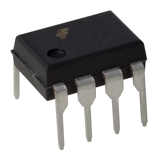 HCPL2601onsemiOPTOISO 2.5KV OPN COLL 8-DIP
 -
 MCT6onsemiOPTOISOLATOR 5KV 2CH TRANS 8-DIP
 -
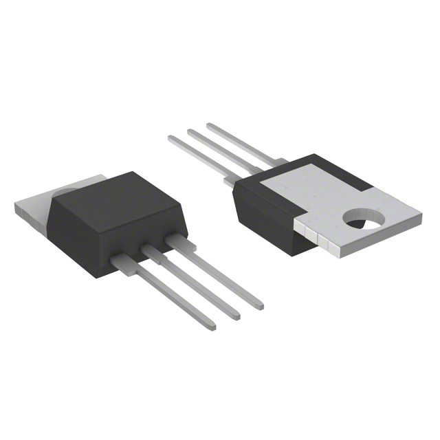 S6008LLittelfuse Inc.SCR 600V 8A TO220
 -
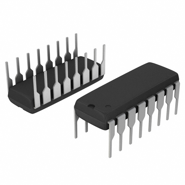 MM74HC4050NonsemiIC BUFFER NON-INVERT 6V 16-PDIP
 -
 MM74HC4049NonsemiIC BUFFER NON-INVERT 6V 16-PDIP
 -
 MM74HC4040NonsemiIC BINARY COUNTER 12-BIT 16DIP
 -
 MM74HC4020NonsemiIC BINARY COUNTER 14-BIT 16DIP
 -
 MM74HC393NonsemiIC BINARY COUNTR DL 4BIT 14MDIP
 -
 MM74HC374NonsemiIC FF D-TYPE SINGLE 8BIT 20PDIP
 -
 MM74HC373NonsemiIC D-TYPE TRANSP 8:8 20-PDIP


