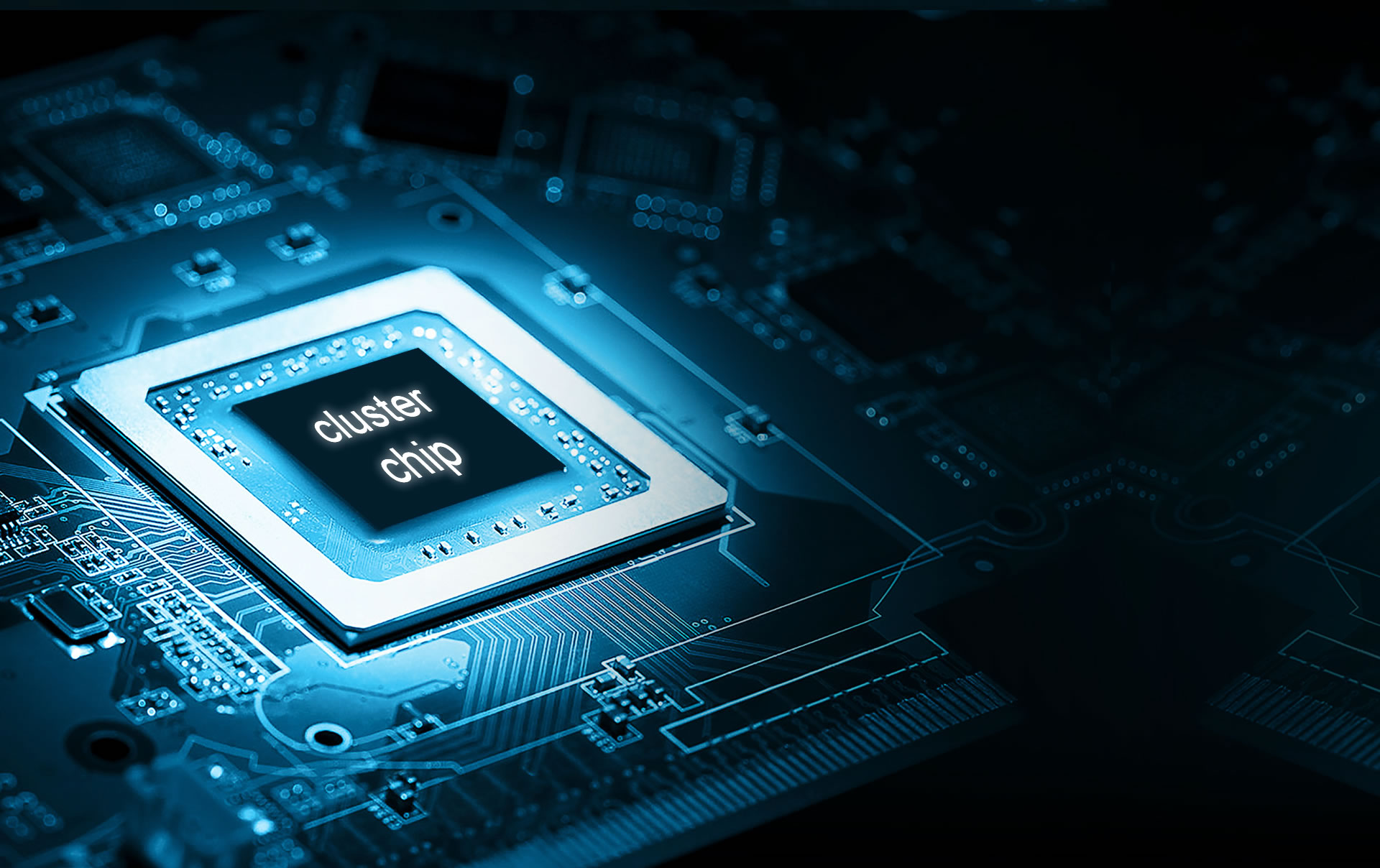
Data-driven insights show a clear shift toward high-voltage SiC solutions in modern power electronics. The , a 3.3 kV SiC MOSFET from Microchip’s MA family, is positioned to deliver low switching losses, robust short-circuit protection, and compact system power density for HV inverter, grid, and industrial applications. This article distills device-level performance, system implications, and practical guidelines to help designers leverage this part effectively. You will see how device traits translate into real-world advantages, from inverter efficiency to system reliability, with practical checkpoints for selection, testing, and procurement.
In today’s HV power landscape, the push from renewables, grid-scale controls, and industrial drives is steering designs toward devices that combine high breakdown capability with tight control of switching losses. The embodies that direction by integrating SiC’s fast switching with robust protection features and an architecture that supports compact form factors. This article synthesizes observed device behavior, system-level implications, and actionable design guidance to help you optimize HV power stages while balancing cost, availability, and lifecycle considerations. The focus remains on delivering data-backed tradeoffs that you can apply directly in HV inverter banks, grid-tollow-through sections, and heavy-duty motor drives.
Background & Market Context for 3.3 kV SiC MOSFETs
’s position within Microchip’s MA Family
The sits in Microchip’s MA family as a high-voltage, die-form factor SiC MOSFET optimized for integration into HV systems. The device emphasizes a Die (DIE) format and is commonly distributed in a waffle-pack packaging suitable for automated assembly in HV power boards. Its positioning within the MA lineup differentiates it from lower-voltage MA family devices through the 3.3 kV rating, enhanced short-circuit robustness, and a design emphasis on high-density HV stages. For your design, this translates into potential reductions in parasitic losses and tighter stacking of inverter legs, while still providing robust protection features compatible with fast-desaturation or overcurrent scenarios. Consider this part when you aim to minimize inverter footprints without sacrificing protective margins in grid-interfacing or utility-scale modules. Link: datasheet reference in the MA family is available as a product profile for quick comparison and procurement planning.
In practical terms, selecting a part from the MA family means weighing die-level characteristics against packaging strategies and supply chain realities. The Die-based approach can offer lower capacitance and faster switching transients in comparison with certain packaged alternatives, contributing to lower switching losses at high frequencies. The waffle-pack packaging supports streamlined thermal paths and easier board-level routing for HV modules, which can translate into improved thermal margins across operating conditions. This positioning also implies careful attention to handling, static discharge precautions, and HPD (high-power device) assembly practices tailored to HV SiC devices. Link: internal references to MA family tradeoffs can guide your architectural decisions during early concept design.
Key specifications and packaging for 3.3 kV operation
The 3.3 kV rating marks the as a candidate for HV stages that require robust breakdown margins while keeping parasitic losses in check. In terms of die-level behavior, expect Rds(on) to reside in the tens of milliohms, contributing to meaningful conduction losses yet enabling a competitive overall efficiency when combined with SiC’s low switching losses. Gate-drive requirements are in the 18–20 V range, which supports strong drive strength for rapid switching without gate overvoltage risks. Device capacitances, including Ciss and Coss, sit in ranges that influence drive current needs, snubber sizing, and EMI budgets. The packaging notes—DIE and thermal performance across -55°C to +150°C, with yield/availability considerations—shape how you plan for thermal management, module integration, and spare parts strategy. For your HV inverter or grid interface, these characteristics help define the isolation margins, gate drive topology, and heat sinking approach you’ll implement. Link: datasheet overview for the provides the official performance envelope and packaging notes you’ll reference during schematic and layout reviews.
Beyond raw ratings, consider reliability and manufacturability implications. The combination of die-level packaging and HV operation often necessitates meticulous layout to minimize parasitic inductance and stray capacitances, as well as careful selection of thermal interfaces to avoid hot spots under peak switching. Yield and supply chain considerations can dictate lifecycle planning, particularly for large module builds. In your project plan, align procurement windows with expected fab-to-packaging throughput and ensure that your BOM accommodates potential obsolescence buffers. Link: internal procurement notes and lifecycle considerations help you map risk and contingency for HV programs.
Comparative landscape in HV SiC MOSFETs
In the 3.3 kV SiC MOSFET space, several options compete on speed, capacitance, and protection features. The differentiates itself by offering a combination of high voltage endurance with a die-based, compact footprint suited for high-integration HV systems. Compared to some alternate 3.3 kV devices, you may observe differences in switching speed and drive requirements, as well as in the available protection schemes. For high-density HV inverters and grid interfaces, the can enable tighter module geometries and improved thermal margins, supporting higher power density with reliable short-circuit protection. This fit is particularly compelling when your system architecture prioritizes footprint reduction, reduced wiring complexity, and predictable performance under abnormal conditions. Link: internal product assessment notes can guide you in comparing protection features and switching characteristics with other HV SiC options.
In short, the sits at a sweet spot for high-integration HV designs that need robust protection, low conduction losses, and a compact form factor. If your system targets solar or wind inverters, HVDC links, or industrial HV drives with tight space and thermal budgets, this device aligns with the design philosophy of minimizing losses while maintaining reliability across a wide operating envelope. Link: internal performance benchmarks for HV SiC devices provide context for your tradeoff studies during design reviews.
Data-Driven Performance Insights for
Electrical performance metrics relevant to high-voltage design
From a design perspective, the delivers key electrical behaviors that influence drive strategies and layout. Switching speed, driven by the device’s capability to transition between on and off states with low energy loss, directly affects efficiency in HV inverters. The device’s gate charge (Qg) and input capacitances (Ciss) inform the drive strength you need from isolated gate drivers and the dead-time you can tolerate without risking cross-conduction. The output capacitance (Coss) and Qgs contribute to switching energy calculations and EMI budgets, shaping the choice of snubbers, gate resistors, and printed-circuit-board trace layouts around the device. In HV inverters and grid applications, these metrics help you balance fast transitions against EMI and thermal activity, guiding you toward a gate-drive scheme that minimizes switching losses while preserving control accuracy. Link: internal device performance summaries provide the baseline values you’ll use for drive optimization and layout planning.
Additionally, the device’s inherent robustness in short-circuit or overload conditions affects how you size protection and define safe operating envelopes. Short-circuit robustness and SOA (Safe Operating Area) margins define whether you can push for aggressive switching schemes or prefer more conservative drive profiles to extend device life under fault events. When you combine this with the high-voltage environment, you can achieve meaningful efficiency gains by optimizing the balance between fast switching (to reduce switching losses) and protective margins that guard against thermal runaway or mechanical stress. Link: internal reliability notes illustrate typical SOA considerations and how protection layers complement device capabilities.
Drive topology selection—whether full-bridge, half-bridge, or multilevel configurations—also interacts with these electrical metrics. The degree of dead-time, the drive voltage window, and the isolation method all influence how effectively you harness the fast-switching nature of SiC devices at 3.3 kV. In your HV system, aligning topology with device capacitances and drive strengths enables lower EMI, tighter control loops, and improved overall efficiency. Link: internal design guidelines outline recommended drive topologies for high-voltage SiC MOSFETs in HV stages.
Reliability and protection considerations at 3.3 kV
Reliability at 3.3 kV hinges on a careful interplay between device capability, thermal management, and protection schemes. The benefits from SiC’s inherent high breakdown strength and fast switching, but you must still manage Safe Operating Area envelopes, ensure robust short-circuit protection, and implement proper thermal paths to prevent hot spots under high current. Heat sinking and effective thermal interfaces—especially in module and multi-die configurations—play a central role in preserving performance over wide operating temperatures. Protection schemes such as TVS clamps, selective clamping, fast fuses, and desaturation monitoring complement the device’s intrinsic robustness, creating a layered defense that reduces the likelihood of catastrophic events and extends device life. Link: internal safety and protection guidelines summarize recommended protection stacks for HV SiC MOSFETs.
Thermal management considerations include recognizing the coupling between conduction losses (Rds(on)) and switching losses. In HV inverters, you can optimize the balance by choosing drive schemes that minimize switching frequency where feasible, while ensuring that conduction losses do not erode efficiency. Proper heat-spreader design and HV-grade cooling solutions help maintain safe operating temperatures across the device’s operating window. Link: internal thermal management references describe practical approaches for HV SiC devices in high-density applications.
Design-for-test and reliability verification should be part of your development plan. You should plan SOA verification, totem-pole drive checks, and targeted thermal cycling to validate behavior under real-world duty cycles. This approach gives you confidence that your HV system will operate within specified margins during long-term operation. Link: internal test plan guidelines provide a structured framework for qualification testing and reliability assessment.
Gate drive integration and drive topology recommendations
Choosing the right gate driver is critical to unleashing the ’s potential in HV systems. You should favor isolated, high-voltage gate drivers with ample drive strength to achieve fast transitions without introducing excessive shoot-through risk. Gate-drive voltage range remains in the 18–20 V area to optimize switching energy while maintaining safe gate integrity. When defining dead-time, aim for a regime that prevents cross-conduction while minimizing reverse recovery currents and EMI. The topology you select—whether a classic full-bridge, half-bridge, or a multi-level arrangement—will influence gate-drive requirements, EMI control strategies, and layout complexity. The drive topology directly affects switching losses and EMI in HV environments, so you should tailor your driver choice to your specific system constraints and regulatory needs. Link: internal drive guidelines provide recommended ranges and best practices for HV SiC MOSFETs in various topologies.
Layout considerations are equally important. Short, low-inductance loop paths around the MOSFETs and the gate driver reduce ringing and overshoot. Proper isolation, consistent grounding schemes, and careful routing around HV traces help you maintain signal integrity and thermal performance. Pair your device with a driver that supports dead-time control, slope compensation where needed, and safeguards against mis-timed switching under fault. Link: internal layout notes outline practical rules of thumb for HV SiC MOSFET installation in power modules.
Applications & System-Level Case Examples
High-voltage inverters for renewables and grid applications
In renewable energy and grid interfacing, the enables compact, efficient HV inverters that can meet stringent efficiency targets while maintaining reliable protection margins. The 3.3 kV rating supports higher line-to-line voltage operation in HVDC and APF (active power filter) contexts, enabling smaller transformer footprints and tighter form factors for offshore or on-site installations. The combination of low conduction losses and fast switching helps reduce overall system losses, contributing to higher grid-constrained efficiencies and improved dynamic response to grid disturbances. In practical terms, expect improvements in overall inverter efficiency, reduced cooling requirements, and potential reductions in system footprint, facilitating easier integration into limited-space substations or multi-port HV systems. Link: internal system-level notes illustrate how device-level improvements cascade into higher-density, higher-efficiency HV modules.
Design teams can leverage the device’s protection features to enhance system reliability, particularly under fault or abnormal conditions. Short-circuit robustness and robust SOA margins allow you to implement aggressive protection strategies with confidence, reducing the likelihood of cascading failures in critical grid interfaces. The net effect is a more resilient HV inverter architecture with a smaller thermal envelope and potentially lower total cost of ownership over the system’s life. Link: internal reliability assessments connect device performance to grid-grade protection architectures for HV deployments.
Industrial drives and heavy-duty motor systems
For industrial motors, pumps, and heavy-duty drives, the supports fast-switching needs while accommodating high current demands and demanding thermal environments. Its 3.3 kV rating aligns with applications that require robust isolation and extended operating margins, contributing to improved motor control performance and dynamic response. The device’s rapid switching reduces switching losses, which can translate into cooler operation and longer motor life when combined with effective thermal management and fan-assisted cooling strategies. In practice, you can achieve higher motor power density and better transient response, enabling smoother torque delivery and reduced acoustic noise in demanding industrial settings. Link: internal case studies illustrate HV motor drive improvements enabled by advanced SiC switching devices.
Protection and fault-mitness remain essential. Short-circuit protection schemes, desaturation monitoring, and fast-acting protective devices complement the ’s intrinsic robustness. These layers help to safeguard gearboxes, bearings, and motors against fault-induced stress, supporting higher uptime and reliability in manufacturing lines and process plants. Link: internal fault-management guidelines explain how to architect multi-layer protection in industrial HV drives.
System-level efficiency and reliability gains
Linking device-level traits to system performance, the ’s combination of high-voltage capability with controlled switching losses contributes to tangible efficiency gains in HV systems. With optimized driver topology, you can realize smaller filter banks, lower EMI budgets, and improved transient response without compromising reliability. The net effect is greater system efficiency, improved thermal margin, and higher reliability across duty cycles that include start-stop, load transients, and regenerative braking scenarios. In summary, this device supports a design philosophy that prioritizes high density, high efficiency, and robust protection in HV applications. Link: internal system-level analyses map device parameters to real-world performance improvements.
Design, Testing & Procurement Guidelines
Selection criteria for
Choosing the involves a rapid, criteria-driven comparison against alternatives. Your quick checklist should include voltage rating (3.3 kV), Rds(on) (tens of milliohms), die vs. packaged options (DIE for density, packaged options for ease of assembly), packaging considerations (waffle-pack suitability for HV modules), availability (lead times and yield), and cost implications. In terms of system-level fit, consider your target HV levels, required switching speed, CSIS/Coss dynamics, and thermal management plan. If you prioritize compactness and high integration for HV inverters or grid enablers, this device is a strong candidate. Link: internal comparison notes summarize the key tradeoffs you’ll use during early-stage design reviews.
Additionally, you should assess supply chain stability and lifecycle considerations. HV SiC devices can be sensitive to obsolescence risk and market fluctuations; incorporate risk buffers and alternate sourcing strategies into your project plan. Understanding packaging implications, parasitic concerns in HV layouts, and procurement lead times helps you avoid schedule slippage and ensure a smooth ramp in manufacturing. Link: internal procurement guidelines provide a structured approach to risk management and lifecycle planning for HV components.
Testing, qualification, and protection strategies
Devise a practical testing plan that includes SOA verification, totem-pole drive checks, short-circuit tests, and thermal cycling to validate behavior under realistic duty cycles. For protection, implement TVS clamps or selective clamping, fast-acting fuses, and desaturation monitoring to complement the device’s intrinsic robustness. A staged qualification approach—starting with benchtop tests, then board-level validation, followed by system-level stress testing—helps you uncover edge conditions and confirm margins before full-scale production. Link: internal test plan templates outline step-by-step procedures for HV SiC MOSFET qualification and protection validation.
Packaging, supply chain, and lifecycle considerations should not be afterthoughts. The DIE/waffle-pack combination demands careful HV layout to minimize leakage and parasitics, particularly in high-frequency or high-density applications. Plan for replacement parts, stock management, and obsolescence risk to minimize production disruption. Ensure your design files reflect packaging constraints and HV layout best practices to streamline manufacturing handoff. Link: internal packaging and lifecycle notes provide actionable guidance for HV device deployment in mass production.
Packaging, supply chain, and lifecycle considerations
Packaging choices influence thermal paths, parasitic behavior, and ease of assembly. The DIE/waffle-pack approach can deliver favorable thermal dissipation and compact module footprints, but it also requires careful handling and HV-aware tooling. From a supply chain perspective, secure reliable distributors and plan for demand variability in HV segments, where lead times may be longer than for mainstream devices. Lifecycle considerations should include obsolescence risk assessment and a contingency plan for alternate supplier availability. Align your procurement plan with expected production volumes, ramp schedules, and warranty expectations to reduce risk. Link: internal packaging and lifecycle notes summarize practical steps for HV device readiness and long-term supply stability.
Key Takeaways
anchors HV power stages with a 3.3 kV SiC MOSFET in Die format, offering high integration potential and robust protection for HV inverters and grid interfaces. This enables higher power density and compact heat management in your designs while maintaining reliability. Link: device-level reference profiles highlight the HV integration benefits.
Expect conduction losses in the tens of milliohms range and fast switching capability that, with proper drive strength and dead-time control, can yield meaningful system-level efficiency gains in high-voltage architectures. Link: drive guidelines summarize how to translate device metrics into efficiency improvements.
Gate-drive strategy, topology choice, and thermal management are pivotal to unlocking the ’s performance. A balanced approach—strong isolated drivers, carefully chosen dead-time, and effective heat sinking—delivers lower EMI and higher reliability in HV modules. Link: topology and layout notes provide practical guidelines for design optimization.
Protection layers—short-circuit robustness, SOA awareness, and fast-fusing strategies—complement the device’s intrinsic strengths, reducing fault risk in demanding HV environments such as renewables, grid controls, and industrial drives. Link: protection guidance maps device features to robust fault-mitigation schemes.
FAQ
What is and what is a 3.3 kV SiC MOSFET?
The is a high-voltage SiC MOSFET designed for 3.3 kV operation, part of Microchip’s MA family. As a DIE-based device, it enables compact HV power stages with strong conduction and switching characteristics suitable for HV inverters, grid interfaces, and industrial drives. A 3.3 kV rating provides substantial headroom for grid-tied and high-efficiency architectures, while SiC’s inherent properties support fast switching and reduced switching losses compared with traditional silicon devices. In practice, you’ll pair this MOSFET with an appropriate isolated gate driver, suitable heat sinking, and protection schemes to achieve high-density HV modules with reliable fault handling. Link: product datasheet overview and family context explain the device’s role in HV power design.
How does the 3.3 kV rating affect HV system design?
A 3.3 kV rating enables higher utilization of HV circuits with fewer devices in parallel per branch, potentially reducing overall topology complexity and parasitics. For your HV inverter or grid interface, this rating supports higher line-to-line voltages, allowing smaller module footprints and tighter integration with transformers and filters. The higher voltage margin also provides room for robust protection margins during fault conditions and improves the Safe Operating Area when combined with well-implemented thermal management. Realizing these benefits requires careful attention to gate drive, dead-time, layout, and cooling to maintain reliability at elevated voltages. Link: internal design guidelines discuss the interplay between HV ratings, protection margins, and thermal management.
What are best practices for gate drive and topology with ?
Best practices emphasize using isolated gate drivers with adequate drive strength to achieve fast, clean transitions while preserving gate integrity. A well-chosen dead-time helps prevent shoot-through without unduly increasing switching losses. The topology you select—be it a classic inverter bridge, a multi-level arrangement, or a high-density half-bridge—should align with the device’s capacitances and drive requirements to minimize EMI and optimize efficiency. Ensure HV layout minimizes parasitic inductance around the MOSFETs and integrates effective thermal paths. Together, these practices enable the SiC device to deliver its low-loss, high-density performance in real-world HV systems. Link: internal drive and topology guidelines provide practical recommendations for HV SiC MOSFET implementation.
What factors influence procurement and lifecycle planning for ?
Procurement considerations include device availability, lead times, pricing, and the risk of obsolescence, particularly in niche HV components. Lifecycle planning should account for replacement parts, supplier diversification, and forecast-driven stocking strategies to mitigate supply disruptions. Packaging choices (DIE/waffle-pack) also impact assembly processes, test flows, and spares management. Aligning your BOM, supplier contracts, and qualification plans with anticipated demand helps ensure timely production and reduces risk in HV programs. Link: lifecycle and procurement notes outline structured approaches to minimize supply risk for HV SiC devices.